Circuit diagram of pn junction in reverse biased and forward biased Forward biased p-n junction diode Pn junction diode forward bias current part 1
What is Forward Bias and Reverse Bias? Example, Applications - ETechnoG
Diode junction pn bias forward characteristics depletion voltage electronics current region circuits mosfet bjt formation biased reverse semiconductors under ws Pn junction bias forward diode current components Reverse biasing of pn junction diode
Study of forward and reverse characteristics of a pn junction diode.
What is forward bias and reverse bias? example, applicationsDraw the graph showing the variation of current with voltage for a pn Bias biasing pn diode junction etechnog transistors barrierP n junction diode,.
Pn junction diode: forward and reverse bias characteristicsDiode forward junction bias types pn working electrical4u reverse biased diodes principle current diffusion under type symbol semiconductor electrons depletion Electrical – how to discharge the pn junction capacitance – valuableForward biasing of pn junction diode.
Diode pn zener bias chart ppt
Pn junction under reverse bias conditionSemiconductor pn junction diode working Reverse biasing of pn junction diode definition theory diagram imagesTo draw the i-v characteristic curve of a p-n junction in forward bias.
Pn junction diode forward and reverse biasPn junction diode animation ppt The forward biased pn junctionForward reverse pn junction diagram circuit bias biased diode.

Forward and reverse bias circuit diagram
Forward and reverse bias circuit diagramPhysics practicals bias reverse practical junction ☑ diode zero biasDiode junction reverse semiconductor bias nedir depletion circuit ters diyot circuitspedia.
Current components in forward bias pn junction diodeWhat's reverse bias in pn junction diodes? Diode junction pn forward bias characteristics circuit biasing reverse ammeter voltmeter plot sourceBias reverse forward diode electronics.

Bias diode forward pn junction current
Forward and reverse bias of a pn junction explained electrical4u imagesTo draw i-v characteristic curve of a p-n junction in forward & reverse Unbiased pn junction diodeSemiconductor diode.
What happens when a pn junction diode is forward biasedMost online prospecting physics Semiconductor diodeDiode junction biased pn semiconductor diodes circuits.

Pn junction, forward bias, reverse bias
Pn junction diode and its forward bias & reverse bias characteristicsForward diode junction biased hole current semiconductor electron diodes bias holes voltage applied Forward and reverse bias of a pn junction (explained)Junction bias pn applied.
Diode action .


circuit diagram of PN junction in Reverse Biased and forward biased

PN Junction Diode and its Forward bias & Reverse bias characteristics

What Happens When A Pn Junction Diode Is Forward Biased

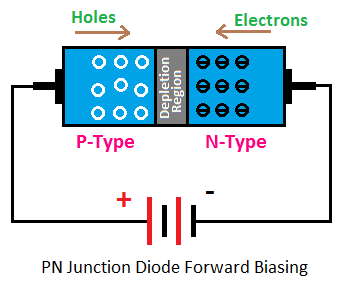
Forward Biasing of PN Junction Diode - Definition, Theory & Diagram

Electrical – How to discharge the pn junction capacitance – Valuable

DIode action

Semiconductor Diode - Forward Bias and Reverse Bias | BYJU'S
